In the vibrant digital world, LED displays are like dazzling canvases that vividly present information to us. But have you ever wondered what kind of "black technology" lies behind these screens, enabling countless pixels to emit light precisely and weave such brilliant images? Today, let's unveil the mystery of SMD packaging technology in LED displays and see how this "little giant" works its magic.
The History of SMD Packaging Development

SMD, which stands for Surface Mounted Device, represents a revolutionary technology in the electronics manufacturing industry. The development history of SMD packaging technology can be traced back to the 1950s, when American microelectronics and electronic component manufacturers began adopting this technology to meet the demand for smaller component packaging.
Over time, SMD packaging technology evolved continuously. In the 1960s, American microelectronics component manufacturers further promoted the use of SMD packaging to meet the growing demand for miniaturization.
In the 1970s, SMD packaging technology saw significant development, with various shapes and sizes of packages emerging, providing technical support for the diversification of electronic products. By the 1980s, SMD packaging technology was widely used in televisions, radios, computers, and many other electronic products, becoming an important pillar of the electronics industry.
In the 1990s, SMD packaging technology made another breakthrough with the emergence of smaller packages such as 0402, 0201, and 01005, further promoting the miniaturization and integration of electronic products.
Entering the 21st century, SMD packaging technology continued to develop, with even smaller packages like 0.3mm x 0.3mm appearing and being widely used in new-generation electronic products such as smartphones and tablets.
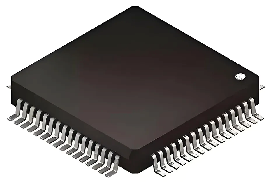
Today, SMD packaging technology includes various common types, such as SOT (Small Outline Transistor) packaging for small transistors, SOD (Small Outline Diode) packaging for small diodes, QFN (Quad Flat No-leads) packaging, BGA (Ball Grid Array) packaging, and DFN (Dual Flat No-leads) packaging.
These diverse packaging types meet the demands of different electronic products in terms of size, shape, and performance, driving continuous innovation and development in the electronics industry.
In LED displays, what is SMD packaging technology?
SMD Packaging Definition
SMD, which stands for Surface-Mounted Device, refers to a packaging technology where LED chips, brackets, and leads are encapsulated into small, leadless LED components. These components are then directly mounted onto a printed circuit board (PCB) using automated pick-and-place machines
Compared to traditional DIP (Dual In-line Package) technology, SMD packaging offers higher integration, smaller size, and lighter weight.
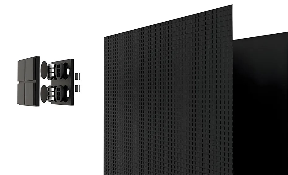
Imagine traditional LED display components as little soldiers wearing heavy armour (leads), requiring drilling and soldering to firmly stand on the circuit board.
In contrast, SMD packaging technology is like dressing these soldiers in lightweight battle gear (leadless design), allowing them to be directly "stick" onto the circuit board. This approach saves space and improves efficiency.
2. Principle of SMD Packaging
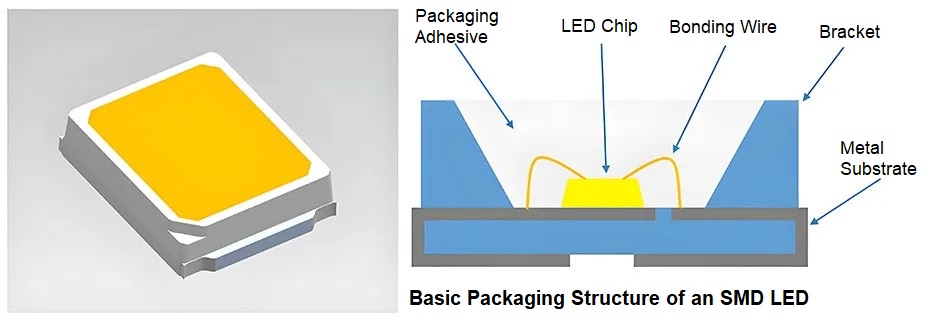
The core of SMD packaging technology lies in "mounting" and "soldering." First, manufacturers encapsulate LED chips, brackets, leads, and other components into small, compact SMD LED packages using precision techniques. These packages do not have long leads; instead, they feature a small metal pad on the bottom, making them well-suited for surface mounting.
Next, automated pick-and-place machines accurately mount the SMD LED packages onto the PCB at predetermined positions and angles. During this process, the machines use high-precision vision systems and mechanical arms to ensure that each LED package is placed precisely in its designated location.
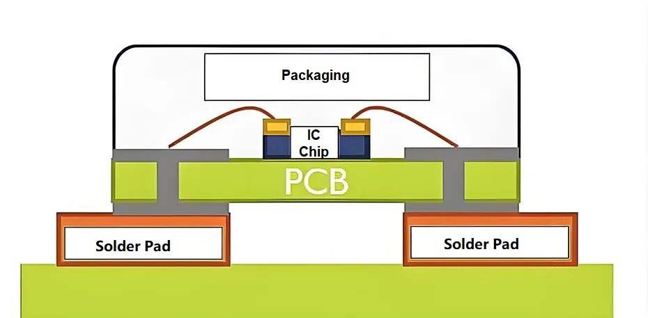
Finally, using high-temperature reflow soldering technology, the SMD LED packages are firmly soldered to the PCB. At high temperatures, the solder melts and flows into the tiny gaps between the LED package and the PCB, creating a stable electrical connection and mechanical fixation. This completes the manufacturing process of each pixel point in the LED display using SMD packaging technology.
3. Features of SMD Packaging
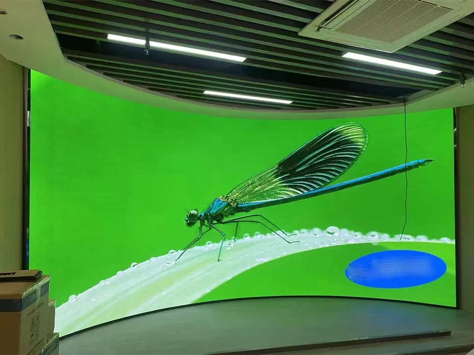
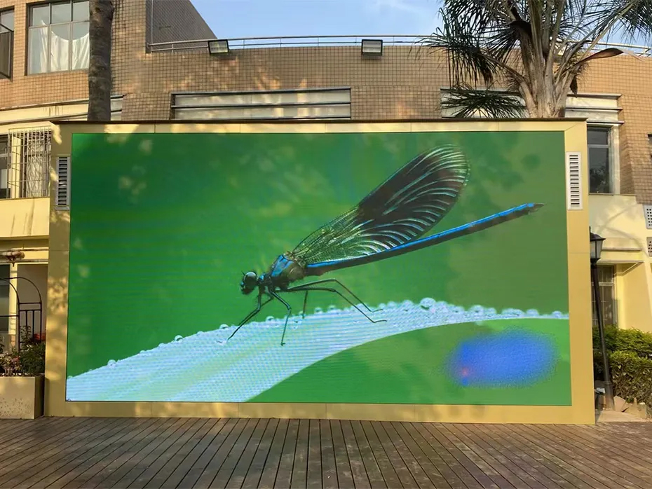
① High Integration and Miniaturization: SMD packaging technology enables LED components to be compact and lightweight, making them ideal for high-density integration. This helps achieve smaller pixel pitches and higher resolutions, enhancing the detail and clarity of the display.
② High Production Efficiency: The use of automated pick-and-place machines significantly boosts production efficiency. Compared to traditional manual
soldering methods, SMD packaging technology allows for faster placement of a large number of LED components, reducing labour costs and production time.
③ Good Thermal Performance: SMD-packaged LED components make direct contact with the PCB, which facilitates effective heat dissipation. Efficient thermal management can extend the lifespan of the LED components and enhance the stability and reliability of the display.
④ Easy Maintenance and Replacement: Since SMD components are mounted directly on the PCB, they are more convenient and quicker to repair and replace. This reduces the maintenance and time costs associated with the display.
4. What Are the Advantages of SMD Packaging?
① High Clarity: Due to the small size of the components, smaller pixel pitches can be achieved, enhancing image detail.
② Low Cost: Automated production reduces manufacturing costs, making the product more affordable.
③ Long Lifespan: Good thermal performance and stable electrical connections extend the lifespan of the display.
5. Which Models of LED Displays Use SMD Packaging Technology?
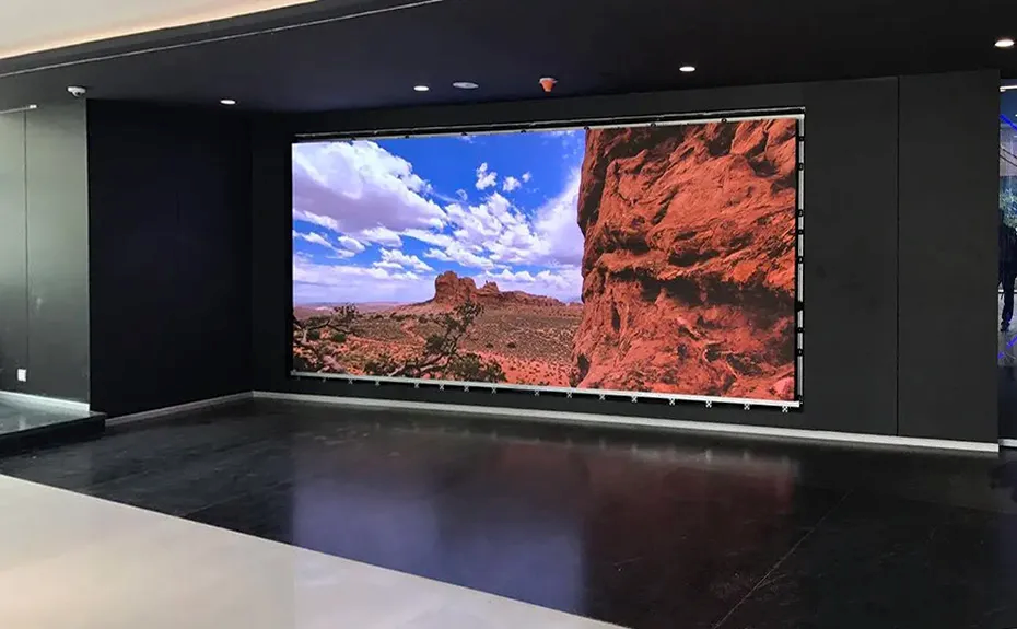
Currently, in the market, many models of LED displays, ranging from indoor small-pitch screens to outdoor full-colour large screens, use SMD packaging technology. Particularly, displays with pixel pitches ranging from P2 to P10 have widely adopted SMD packaging technology due to its maturity and cost-effectiveness, making it the mainstream choice.
6. What Are the Main Application Areas for LED Displays Using SMD Packaging Technology?
① Commercial Advertising: Large advertising screens in public places such as shopping malls, airports, and subway stations.
② Conferences and Exhibitions: Stage background screens and information display screens at various exhibitions and conference venues.

③ Sports Venues: Audience display screens in large sports venues such as soccer stadiums and basketball arenas.

④ Outdoor Media: Outdoor display applications such as cityscape lighting and highway billboards.
SMD packaging technology, as the "little giant" behind LED displays, has become an indispensable part of modern electronics manufacturing due to its compact size, efficient production, excellent heat dissipation, and ease of maintenance. It has not only accelerated the rapid development of LED display technology but also provided us with clearer, more vibrant, and dynamic visual experiences. With continuous technological advancements, SMD packaging technology is expected to keep shining and creating more miracles in the future.